Collaboration

AMOLF, CWI, and DIFFER launch HELIOS project with NWO-I funding

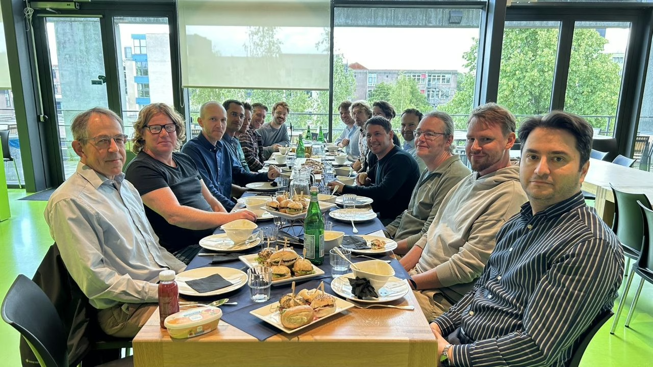
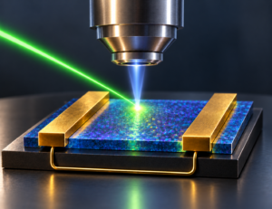
An AMOLF collaboration with CWI and DIFFER has received funding from NWO-I to launch a joint project: HELIOS: AI-guided materials discovery facility for solar energy materials. On Friday, May 23rd, representatives from the three institutes gathered for the kick-off meeting to discuss the roadmap toward developing a highly efficient multilayered halide perovskite solar cell.

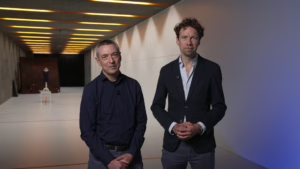
HELIOS kick-off meeting at AMOLF

NWO-I funds proposals such as HELIOS to strengthen connections between its institutes and to support research that aligns with and advances each institute’s mission.

In the HELIOS project, AMOLF will contribute its expertise in fundamental research on functional materials. CWI will lead the AI efforts, while DIFFER brings in strong systems engineering, machine learning, and data management capabilities.

Project leader Erik Garnett notes that the project faces a variety of practical challenges:

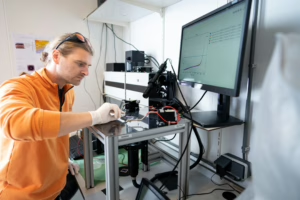
“A regular solar cell has five layers, but we’re aiming for twenty layers that interact perfectly with each other.” He adds that these layers must not only function well individually but also integrate seamlessly. “For example, processing for one layer may affect the layer beneath it.” AMOLF researchers will take on this challenge, along with others that arise during the development of the solar cell.”

The HELIOS solar cell material will operate as a learning system. CWI researchers will implement AI technology to guide experimental choices. Coupled with the researchers’ scientific intuition, this approach is expected to accelerate progress significantly.

The project also involves a substantial number of AMOLF support staff. Erik highlights the contributions from several departments:

  • ICT is involved due to the large volume of data generated;
  • Electrical engineering expertise is required to build custom complex electronic interfaces;
  • The design department is responsible for the mechanical design of robotic interfaces;
  • The precision manufacturing department will make custom parts for automated interfaces;
  • Software engineers will to build and maintain automated systems.

The total budget for HELIOS is € 3.710.000 and the project is expected to run for 5 years.

Do you want to find out more about sustainable energy materials? Then, have a look at our Sustainable Energy Materials webpage.
Share article
What's happening

Most recent news items

All news items
Joining forces to study perovskite interfaces
People and recognition

Joining forces to study perovskite interfaces

AMOLF group leaders Professor Wiebke Albrecht and Professor Bruno Ehrler have received an NWO ENW-M2 grant for their joint research project, The Dynamic Atomic Interface between Halide Perovskites and Metals. The insights gained will pave the way for sustainable, high-performance solar energy and information technology. Wiebke and Bruno will each hire a PhD student for this project. The grant amounts to €800.000.

Read news item
Wim Noorduin and Arian van Asten presenting their scientific journey
People and recognition

Wim Noorduin and Arian van Asten presenting their scientific journey

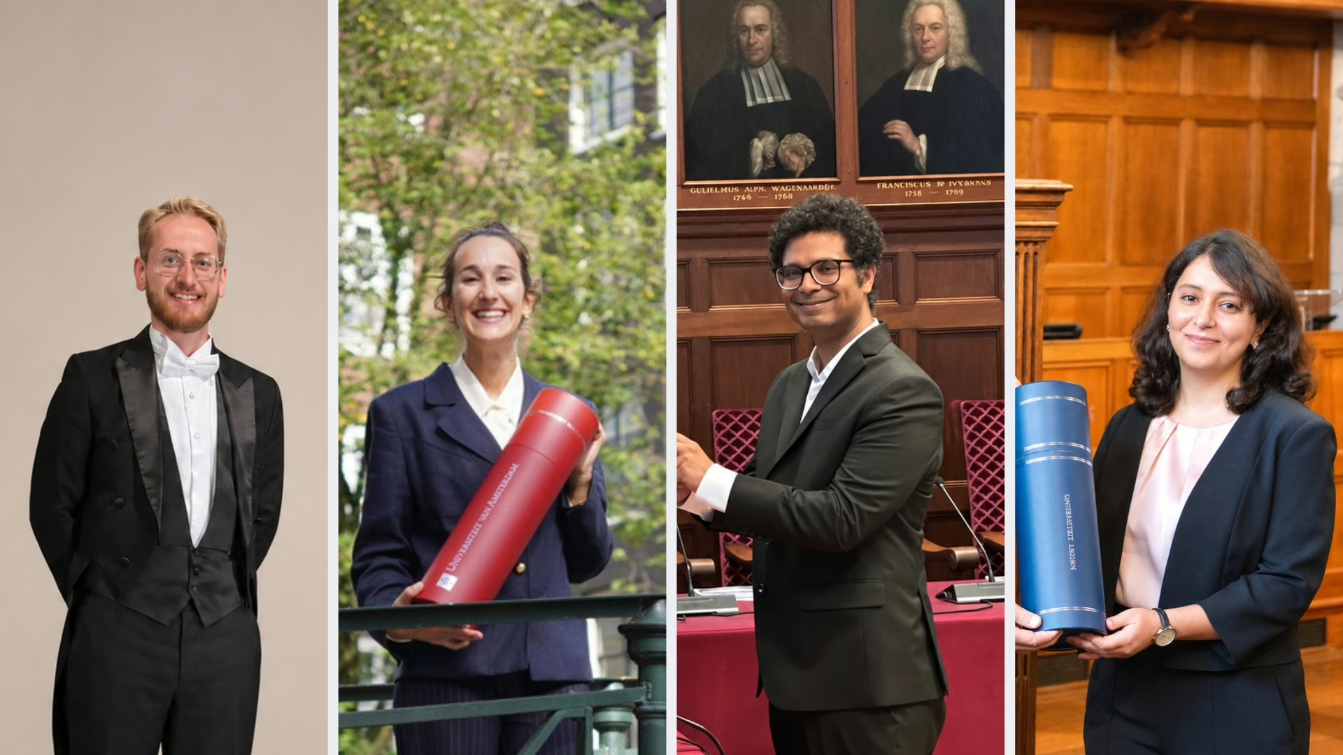
On October 8, Professor Wim Noorduin and his collaborator Professor Arian van Asten (University of Amsterdam) presented their scientific journey in a video to the audience at the ‘Avond van Wetenschap en Maatschappij’. They did so alongside the other nominees for the Huibregtsen Prize.

Read news item
Natural phenomena ‘hyperuniform disorder’ enables highly efficient, thin silicon solar cells
Research highlights

Natural phenomena ‘hyperuniform disorder’ enables highly efficient, thin silicon solar cells

Silicon solar panels are rigid and heavy, and many rooftops cannot support them. This creates a need for thin, flexible solar cells that can be integrated into building materials. However, making silicon solar cells thinner makes it harder to trap light inside the material. Researchers in the 3D Photovoltaics group found a fascinating way to overcome this challenge using a phenomenon called hyperuniform disorder. They publish their findings in the journal ACS Photonics.

The researchers were able to make highly efficient silicon solar cell materials that are 30 times thinner than conventional ones. They managed to do this by integrating a layer of nanometer sized structures on top of the material. Up close, this pattern looks random, but it is remarkably when you step back: no clumps, no gaps, and no repeating pattern. This is called hyperuniform disorder (or HUD).

Read news item
Stay informed

Get the latest research highlights, events, and news from our institute delivered to your inbox