
Topological insulators: special electronics
Verhagen and his collaborator Kobus Kuipers from TU Delft were inspired by electronic materials, where so-called topological insulators form a new class of materials with remarkable behavior. Where most materials are either conductive for electrons or not (which makes them an insulator), topological insulators exhibit a strange form of conduction. “The inside of a topological insulator does not allow electron propagation, but along the edge, electrons can move freely”, says Verhagen. “Importantly, the conduction is ‘topologically protected’; the electrons are not impacted by disorder or imperfections that would typically reflect them. So the conduction is profoundly robust.”
Translation to photonics
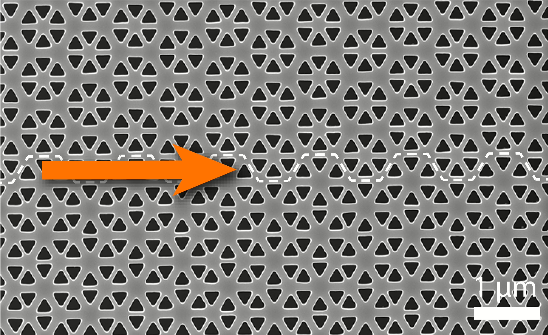
In the past decade, scientists have tried to find this behavior for the conduction of light as well. “We really wanted to accomplish topological protection of light propagation at the nanoscale and thus open the door to guiding light on optical chips without it being hindered by scattering at imperfections and sharp corners”, says Verhagen. For their experiments, the researchers used two-dimensional photonic crystals with two slightly different hole patterns. The ‘edge’ that enables light conduction is the interface between the two hole patterns. “Light conduction at the edge is possible because the mathematical description of light in these photonic crystals can be described by specific shapes, or more accurately by topology,” Kuipers says. The topology of the two different hole patterns differs and precisely this property allows light conduction at the boundary, similar to electrons in topological insulators. Because the topology of both hole patterns is locked, light conduction cannot be revoked; it is ‘topologically protected’.”
Imaging topological light
The researchers managed to image light propagation with a microscope and saw that it behaved as predicted. Moreover, they witnessed the topology, or mathematical description, in the observed light. Kuipers: “For these light waves the polarization of light rotates in a certain direction, analogous to the spin of electrons in topological insulators. The spinning direction of light determines the direction in which this light propagates. Because polarization cannot easily change, the light wave can even flow around sharp corners without reflecting or getting scattered, as would happen in a regular waveguide.
Technological relevance
The researchers are the first to directly observe the propagation of topologically protected light on the technologically relevant scale of nanophotonic chips. By purposely using silicon chips and light of a similar wavelength as used in telecommunication, Verhagen expects to increase the application prospects. “We are now going to investigate if there are any practical or fundamental boundaries to topological protection and which functionalities on an optical chip we could improve with these principles. The first thing we are thinking of is to make the integrated light sources on a photonic chip more reliable. This is important in view of energy-efficient data processing or ‘green ICT’. Also, to efficiently transfer small packages of quantum information, the topological protection of light can be useful.
Reference
N. Parappurath, F. Alpeggiani, L. Kuipers, and E. Verhagen, “Direct observation of topological edge states in silicon photonic crystals: Spin, dispersion, and chiral routing,” Science Advances 6, eaaw4137 (2020).