Research highlights

Less can be more: semiconductor nanowires for flexible photovoltaics

Capturing and manipulating light at nanoscale is a key factor to build high efficiency solar cells. Researchers in the 3D Photovoltaics group have recently presented a promising new design. Their simulations show that vertically stacked nanowires on top of ultrathin silicon films reduces the total amount of material needed by 90% while increasing the efficiency of the solar cell. These promising simulation results are an important step towards new generation solar cells that are used in myriad ways in our buildings and landscape. The results have been published on May 23rd in Optics Express.

How does it work
A fascinating strategy to reduce both cost and rigidity is to combine ultrathin silicon photovoltaic films with semiconductor nanowire solar cells. The mechanical flexibility and resilience of micrometer thin cells make them well suited to apply on curved surfaces. The idea is to optically couple the two materials stacked on top of each other as a tandem cell: a Gallium Arsenide (GaAs) nanowire array on top of an ultrathin silicon (2um-thick) film. GaAs vertical  nanowires are well-known semiconductor components in photovoltaic applications.

Earlier experimental research in the 3D photovoltaics group has shown that such nanowires are able to absorb light ten to hundred times their geometrical cross section. Silicon, the second material in the tandem cell, is a highly desirable component thanks to the mature understanding of its optical and electronic properties as well as its widely available fabrication technologies. The challenge researchers typically encounter when trying to downscale silicon to a few micrometers in thickness is that it compromises the solar cell’s performance due to poor absorption of infrared light. Light management strategies are therefore needed to compensate. The research team decided to add  vertically standing nanowires on top of silicon film and thereby make it  up to four times more efficient in trapping infrared light in the silicon bottom cell.

Reference
Nasim Tavakoli and Esther Alarcon-Llado, Combining 1D and 2D waveguiding in an ultrathin GaAs NW/Si tandem solar cell, Optics Express, 27, A909-A923 (2019).
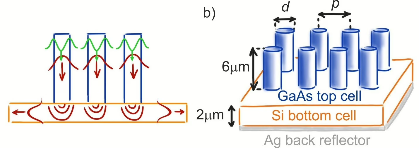
Caption: Optically coupled tandem of GaAs nanowires (6um tall) on silicon ultrathin film (2um). Sunlight is efficiently absorbed in each nanowire, and the array will transmit infrared light to be trapped into silicon film.
Share article
What's happening

Most recent news items

All news items
Joining forces to study perovskite interfaces
People and recognition

Joining forces to study perovskite interfaces

AMOLF group leaders Professor Wiebke Albrecht and Professor Bruno Ehrler have received an NWO ENW-M2 grant for their joint research project, The Dynamic Atomic Interface between Halide Perovskites and Metals. The insights gained will pave the way for sustainable, high-performance solar energy and information technology. Wiebke and Bruno will each hire a PhD student for this project. The grant amounts to €800.000.

Read news item
Wim Noorduin and Arian van Asten presenting their scientific journey
People and recognition

Wim Noorduin and Arian van Asten presenting their scientific journey

On October 8, Professor Wim Noorduin and his collaborator Professor Arian van Asten (University of Amsterdam) presented their scientific journey in a video to the audience at the ‘Avond van Wetenschap en Maatschappij’. They did so alongside the other nominees for the Huibregtsen Prize.

Read news item
Natural phenomena ‘hyperuniform disorder’ enables highly efficient, thin silicon solar cells
Research highlights

Natural phenomena ‘hyperuniform disorder’ enables highly efficient, thin silicon solar cells

Silicon solar panels are rigid and heavy, and many rooftops cannot support them. This creates a need for thin, flexible solar cells that can be integrated into building materials. However, making silicon solar cells thinner makes it harder to trap light inside the material. Researchers in the 3D Photovoltaics group found a fascinating way to overcome this challenge using a phenomenon called hyperuniform disorder. They publish their findings in the journal ACS Photonics.

The researchers were able to make highly efficient silicon solar cell materials that are 30 times thinner than conventional ones. They managed to do this by integrating a layer of nanometer sized structures on top of the material. Up close, this pattern looks random, but it is remarkably when you step back: no clumps, no gaps, and no repeating pattern. This is called hyperuniform disorder (or HUD).

Read news item
Stay informed

Get the latest research highlights, events, and news from our institute delivered to your inbox