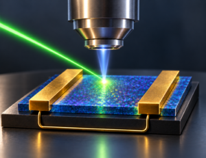
Some of the most exciting materials in modern science come in the form of stacked, thin sheets. Here, “thin” really means thin: each sheet can possibly reach the thickness limit of a single layer of atoms. Since the height of these materials is negligible, they are called 2D materials. They can be thought of as a stack of sticky notes: each sheet is firmly held together on its own, but the layers only gently stick to one another, making them easy to peel apart. Interestingly, due to the workings of quantum mechanics, the individual atom-thin layers show remarkable properties that the original, much thicker crystals that they come from, do not exhibit. For example, the layers can show very low electrical resistance, have strong interaction with light, or even have flexible but resistant mechanical properties.
Cracks in the paint
However, there is a catch. Obtaining a usable sheet of super thin material has been a real challenge. The traditional method, used for the last 22 years, involves pressing ordinary adhesive tape onto a crystal and peeling it off. If you have ever accidentally removed some paint by peeling off painter’s tape, and looked at what was left on the tape, you will realize what the problem is. While the method works, it tends to crack the material, leaving you with thin but tiny flakes. In the 2D materials case, these flakes are smaller than the width of a human hair – far too small for most practical devices.
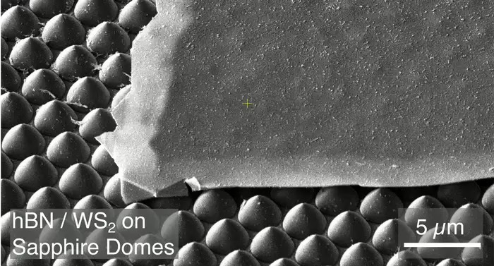
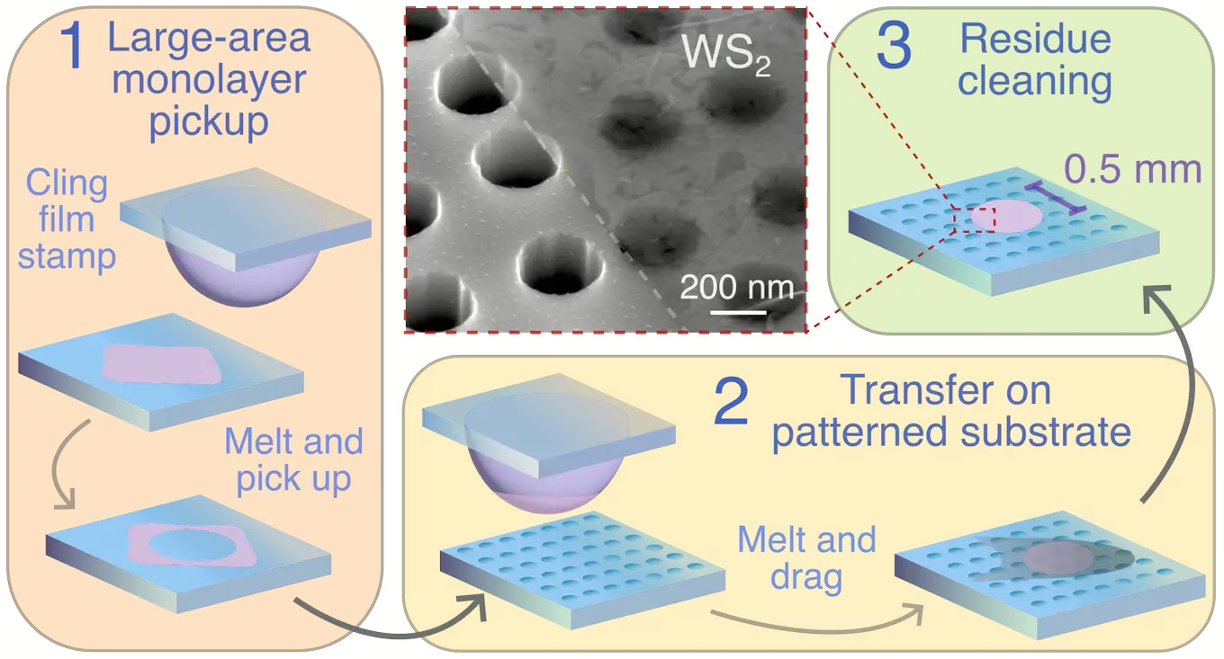
A new approach using gold films – aptly called gold-assisted exfoliation – was discovered in 2018 and was a big step forward. It allowed researchers to peel off much larger, centimeter-scale sheets and transfer them to flat glass surfaces. However, a new problem emerged: most real devices aren’t flat. They have patterns on them – ranging from tiny electrical contacts to optical coatings and textured surfaces. The “paint cracking” problem reappeared: So far, nobody had figured out how to place these large, ultra-thin sheets onto such accentuated surfaces without damaging the sheets.
An unexpected tool
The problem of transferring large enough thin sheets of material is exactly what the new research solves – and an ordinary kitchen material did the trick. It turned out the best way to transfer the layers was by using ordinary kitchen cling film, exactly what you buy in the supermarket and use to wrap around your left-over pizza.
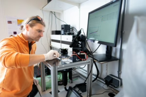
University of Amsterdam (UvA) PhD candidate Bernardo Dias, first author of the paper, explains: “When I started at our research group 3 years ago, I quickly realized how difficult device fabrication with 2D materials was. Assembling a full device was probabilistic – sometimes the 2D material just didn’t stick to the surface – and in the end you got a tiny, micrometer-sized device. Encouraged by my supervisor, Jorik van de Groep, I went on a detour to find a better method, and it turned out cling wrap has just the right properties to handle these delicate materials gently and effectively.”
Jorik van de Groep, head of the 2D Nanophotonics group at the UvA-Institute of Physics, adds: “The discovery to use cling film for this application came by total accident. We were trying to replicate results from a research group in Japan, but it turned out kitchen cling film in Europe is made of a different polymer. We observed that the polymer used here melts at 120°C, while theirs did not. This property turned out to be the defining factor in successful 2D material transfer: we could simply melt the cling film on top of the material to make it stick.”
Symbiotic collaboration
The team that developed the new technique was fully based at the Amsterdam Science Park, but involved experts from several different institutes. Van de Groep: “The collaboration was remarkable. The project was managed at the UvA-Institute of Physics but we had collaborations with the chemists at UvA’s Van ‘t Hoff Institute for Molecular Sciences, nanolithographers at ARCNL, and complex matter scientists at AMOLF. The end result was only possible through a symbiotic collaboration among all.”
Dias also enjoyed the large collaboration: “It was an extremely rewarding experience – I got to learn a lot and I am quite happy to see people in our groups using this technique reliably to explore new science with it.”
New goals within reach
The new technique should have a wide array of potential applications. It does not just allow the “gift-wrapping” of large, accentuated materials by single layers of a material, it turns out that the process also improves how the material emits light. With large-area 2D material transfer now within reach, applications that were previously difficult to pursue become feasible. Large-scale fabrication of 2D material-based transistors, or the development of ultra-thin optical elements such as lenses and modulators, are now more accessible avenues for researchers and engineers to explore.
The opportunities are not purely technological. Stacking thin materials on top of one another can give rise to properties that neither material has on its own, making them a rich platform for studying novel physics in condensed matter systems. Whether the goal is to build the next generation of devices or to explore new quantum phenomena, this technique makes both a little more within reach.
Contact
For more information about this research, please contact Professor Esther Alarcón-Lladó.
Publication
Large-Area Deterministic Stamping of 2D Materials on Patterned Surfaces, Bernardo S. Dias, Reynolds Dziobek-Garrett, Gabriella Mentasti, Abhishek Gupta, Alexander Lambertz, Esther Alarcón-Lladó, Peter Schall, Roland Bliem and Jorik van de Groep. ACS Nano 6c04231 (2026).