Focusing light is important for various technological applications on photonic chips, such as quantum communication, optical sensors, and on-chip lasers. “Until now, we knew two general strategies to concentrate light: it can be done using optical cavities, or with waveguides that compress the light like a funnel,” says AMOLF group leader Ewold Verhagen. “The first method uses resonance, which limits the focusing or concentration of light to a specific wavelength. The second method works, similar to a traditional lens, only in a device much larger than the wavelength of the light used.”
Blocking light
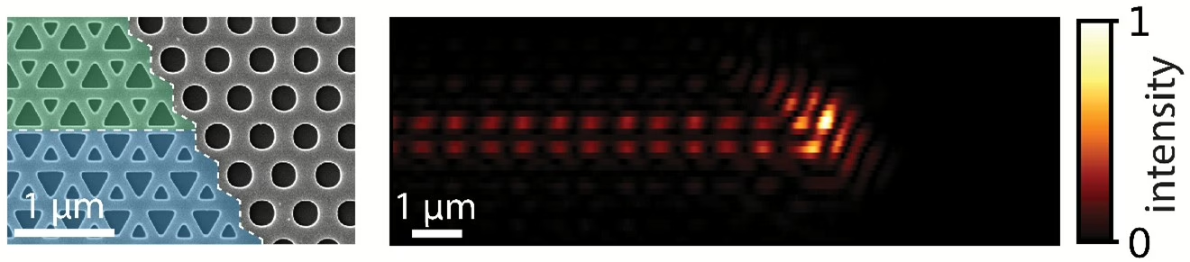
A theoretical idea from researchers at Cornell University, led by Gennady Shvets, pointed to the new method that PhD candidate Daniel Muis and his colleagues have now demonstrated for the first time. An important aspect of the method is the so-called topology of the physical system. Daniel explains: “We use photonic crystals, which are slabs of silicon with a regular pattern of very small holes, which forbid light propagation in the silicon slab, in principle. But, when we place two of these crystals with a mirrored pattern next to each other, a waveguide is created at their boundary; the light can only move along the boundary. What makes this design special is that the conduction of light is ‘topologically protected,’ meaning that scattering or reflection of light by imperfections in the crystal is suppressed.”
The researchers wondered what would happen if they abruptly ended such a waveguide, with a ‘wall’ of material that light cannot pass through. “Since the light has nowhere to go and reflections are suppressed, it should accumulate in front of that wall,” says Daniel. “The light does eventually bounce back through the waveguide, but only after a delay. This results in a local amplification of the light field.”
Light concentration
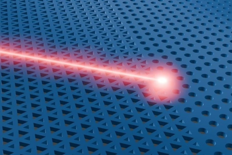
The groups of Ewold Verhagen at AMOLF and Kobus Kuipers at TU Delft decided to verify the predictions in an experiment together with the researchers from Cornell. The topological waveguides were made on a silicon chip at AMOLF. To visualize the predicted accumulation of light within the photonic crystal, Daniel used a unique microscope at TU Delft that scans light fields via an ultra-thin needle above the surface of the crystal. This microscope can localize light intensity on a scale about a thousand times smaller than the thickness of a human hair. “We indeed saw a clear amplification of the light field at the end of the topological waveguide. Interestingly, this only happened when the ‘wall’ terminating the waveguide was placed at a certain angle. This was exactly what our partners at Cornell had predicted,” says Daniel. “It proves that the light amplification is related to the topological suppression of back reflection. The light amplification is concentrated in a very small volume, as small as the wavelength of the light itself. A major advantage of this method is that it is inherently broadband: it works for multiple different wavelengths.”
The article in Science Advances, with equal contributions from Daniel and his Cornell colleague Yandong Li, can be read as a recipe for further research or applications of this form of light amplification on a chip. The demonstrated mechanism should also apply to any other type of wave in a structured medium, including sound waves or even electrons in specific crystals. Daniel: “For a next step, it would be interesting to use a pulsed laser to look at the time interval in which the light continues to accumulate, to see how much the field amplification can be maximized, and to use it for applications in light manipulation on optical chips.”
Reference
Daniel Muis, Yandong Li, Rene Barczyk, Sonakshi Arora, L. Kuipers, Gennady Shvets, Ewold Verhagen, Broadband localization of light at the termination of a topological photonic waveguide, Science Advances, April 18 (2025). Find out more in the research paper:
“Broadband localization of light at the termination of a topological photonic waveguide”
Learn more
Curious about research in the group of Ewold Verhagen? Have a look at our Photonic Forces research group.