Research highlights

Tiny thermometers: measuring heat flow dissipating via nanoparticles

How do materials behave when heated with light at the scale of billionths of a meter? Researchers at AMOLF and Kobe University have developed a method to watch this process with nanometer precision. Their work, recently published in ACS Photonics, reveals how silicon nanoparticles heat up under laser light and how heat escapes from the surfaces. This breakthrough opens new doors for improving electronics, solar cells, and catalysts by giving scientists a sensitive tool to measure and control heat flow at the nanoscale.

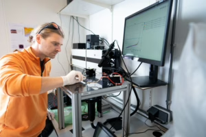
Researcher Saskia Fiedler in the electron microscopy lab. Photo: AMOLF

Building a nanoscale thermometer 

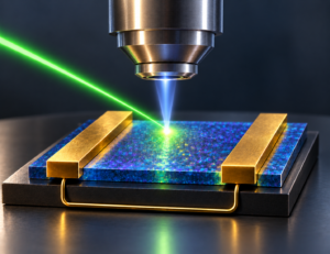
The research team, led by first author Saskia Fiedler and group leader Albert Polman, designed a technique that combines laser heating with cathodoluminescence spectroscopy. Cathodoluminescence is the process where light is emitted when a material is struck by an electron inside a scanning electron microscope (SEM). By monitoring the light emitted by nanoparticles as they heat up, the researchers can directly map temperature changes across a single particle with unprecedented accuracy. 

Challenges in the lab 

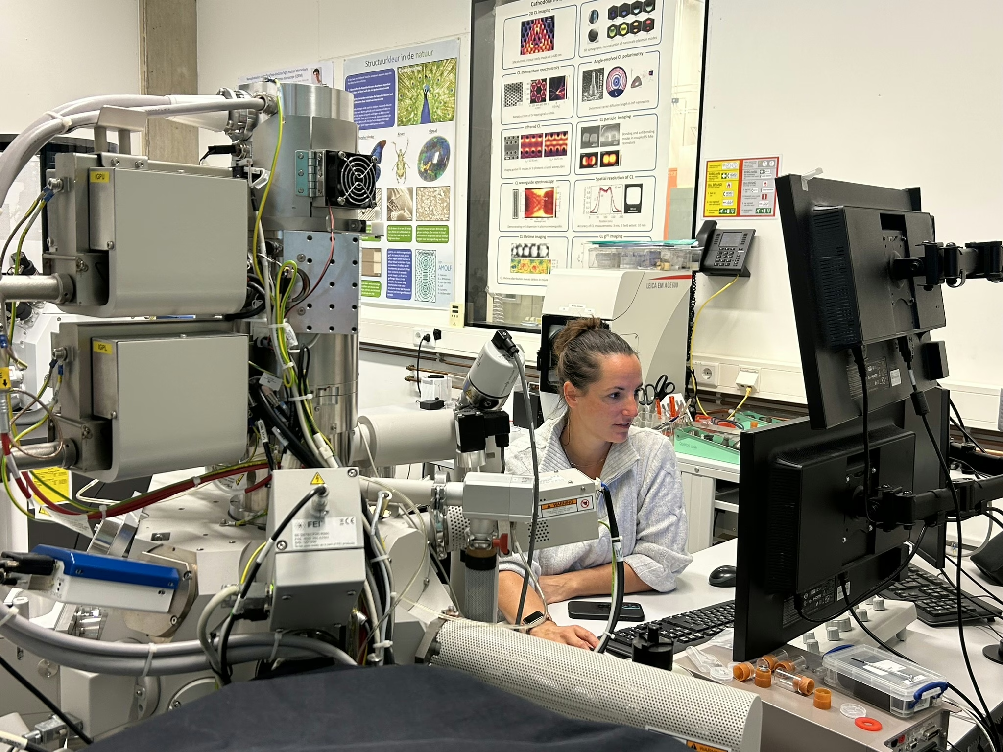
Developing this method was not straightforward. One of the biggest hurdles came from the experimental setup itself. Some optical components in the microscope produced unwanted fluorescence when exposed to the laser, creating strong background signals that masked the actual data. “At first, it was very frustrating,” recalls Saskia. “The signal we wanted to measure was buried under this noise.” By carefully replacing components and redesigning parts of the experiment, the team managed to filter out the background, making the real signal visible. 

Watching heat in action 

With the refined setup, the researchers heated silicon nanospheres up to nearly 600 degrees Celsius. As the temperature rose, the color of the emitted light shifted in a predictable way, much like glowing coals changing color as they get hotter. By analyzing these shifts, the scientists could determine not only how hot the nanoparticles became, but also how heat flowed out through their tiny contact points with the surrounding environment. 

Why this matters 

Understanding heat at the nanoscale is crucial for many modern technologies. In electronic circuits, excess heat can limit performance and lifespan. In solar cells, managing heat flow can boost efficiency. And in catalysts, precise control of local temperatures can make chemical reactions more effective. The new nanoscale thermometer developed by the team provides a tool to address these challenges across different fields. 

Looking ahead 

The study demonstrates a proof-of-principle for a powerful new measurement technique. Albert: “What excites me most is that we now have a way to look at temperature with nanometer precision. This gives us a window into processes that were invisible before.”  

Learn more and read publication 

Reference

Saskia Fiedler, Loriane Monin, Hiroshi Sugimoto, Minoru Fujii, Wiebke Albrecht and Albert Polman, Nanoscale Heat Flow and Thermometry in Laser-Heated Resonant Silicon Mie Nanospheres Probed with Spatially Resolved Cathodoluminescence Spectroscopy, ACS Photonics, September 19 (2025) 

Share article
What's happening

Most recent news items

All news items
Joining forces to study perovskite interfaces
People and recognition

Joining forces to study perovskite interfaces

AMOLF group leaders Professor Wiebke Albrecht and Professor Bruno Ehrler have received an NWO ENW-M2 grant for their joint research project, The Dynamic Atomic Interface between Halide Perovskites and Metals. The insights gained will pave the way for sustainable, high-performance solar energy and information technology. Wiebke and Bruno will each hire a PhD student for this project. The grant amounts to €800.000.

Read news item
Wim Noorduin and Arian van Asten presenting their scientific journey
People and recognition

Wim Noorduin and Arian van Asten presenting their scientific journey

On October 8, Professor Wim Noorduin and his collaborator Professor Arian van Asten (University of Amsterdam) presented their scientific journey in a video to the audience at the ‘Avond van Wetenschap en Maatschappij’. They did so alongside the other nominees for the Huibregtsen Prize.

Read news item
Natural phenomena ‘hyperuniform disorder’ enables highly efficient, thin silicon solar cells
Research highlights

Natural phenomena ‘hyperuniform disorder’ enables highly efficient, thin silicon solar cells

Silicon solar panels are rigid and heavy, and many rooftops cannot support them. This creates a need for thin, flexible solar cells that can be integrated into building materials. However, making silicon solar cells thinner makes it harder to trap light inside the material. Researchers in the 3D Photovoltaics group found a fascinating way to overcome this challenge using a phenomenon called hyperuniform disorder. They publish their findings in the journal ACS Photonics.

The researchers were able to make highly efficient silicon solar cell materials that are 30 times thinner than conventional ones. They managed to do this by integrating a layer of nanometer sized structures on top of the material. Up close, this pattern looks random, but it is remarkably when you step back: no clumps, no gaps, and no repeating pattern. This is called hyperuniform disorder (or HUD).

Read news item
Stay informed

Get the latest research highlights, events, and news from our institute delivered to your inbox