Nature Synthesis. This breakthrough could make optoelectronics more efficient by controlling the crystal structure and reducing the number of defects at the nanoscale.
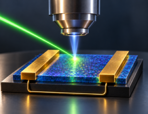
The team focused on a material called metal halide perovskites, known for its ability to absorb sunlight efficiently and its use in devices like LEDs, semiconductors and solar cells. Making these materials with one single orientation (with highly ordered grains) has been a challenge. Up to date this has mainly been used in the polycrystalline form, so in a non-ordered fashion. This can limit their use in applications, such as LEDs, where high order and low density of defects are needed. Normally, these highly ordered semiconductors require high processing temperatures. But in this new process, the researchers skip the heat and built up the material layer by layer using a pulsed laser.
Getting the structure right
“It’s all about getting the structure right,” says Monica Morales-Masis, who leads the work under the ERC StG CREATE project. “A perfectly ordered structure in the material is essential for creating devices that are efficient and reliable. The resulting material is stable for over 300 days and offers great potential for applications like solar panels and advanced electronics. This innovation not only helps us in creating greener, more cost-effective technologies but also paves the way for new scientific discoveries in materials research.”
Interdisciplinary collaboration
This research highlights the power of interdisciplinary collaboration, involving contributions from synthesis, theory, and advanced characterisation. The synthesis and core experimental work were performed at the University of Twente, with theoretical insights provided by Prof Dr Linn Leppert and her team at UT. Advanced characterisation was conducted in partnership with AMOLF, the University of Oxford, and other institutions, showcasing a global network of expertise.
In this work, Nikolai Orlov of AMOLF’s Nanoscale Solar Cells Group provided electron backscatter diffraction (EBSD) images of the halide perovskite films deposited by pulsed laser deposition to confirm that they grew epitaxially on cubic KCl lattice-matched substrates. AMOLF Group Leader Erik Garnett: “In plain English, this means that a laser was used to deposit atoms of halide perovskite onto a salt crystal and the atomic positions of the resulting film matched exactly with the underlying substrate. Our EBSD detector, which was developed together with our industrial partners EDAX and ASI, is able to image this crystal orientation because of its extreme sensitivity.”
More information
The researchers published their work in an article in the scientific journal Nature Synthesis. This work is financed by the ERC StG CREATE project as well as an OTP project at AMOLF. The results will be applied in a follow up project within the National Growth Fund Program SolarNL for the large-scale production of solar cells and solar panels in the Netherlands.
You can find more information about this project in this press release of the University of Twente. If you have questions, you can contact Erik Garnett (email: E.Garnett@amolf.nl) .