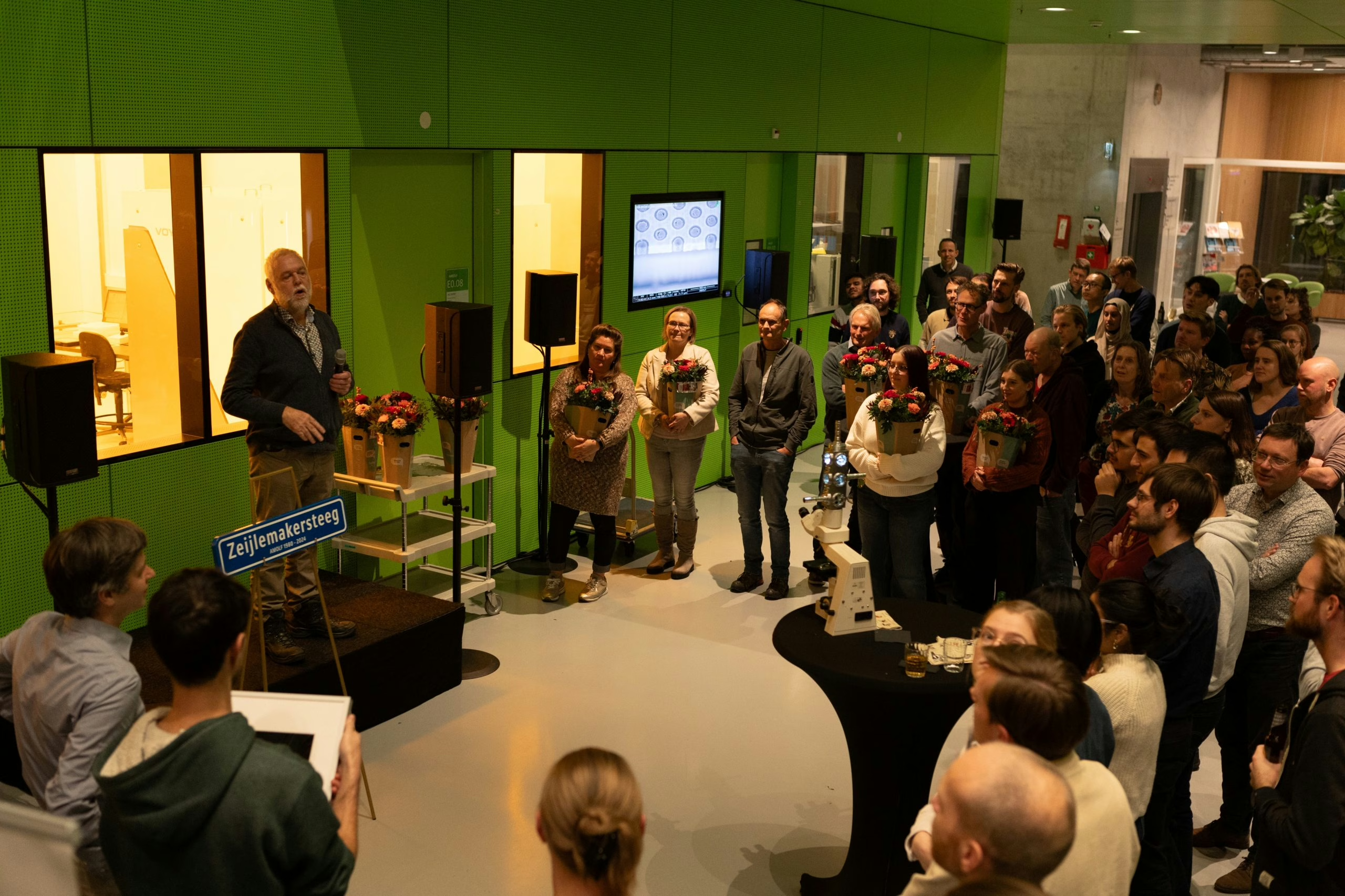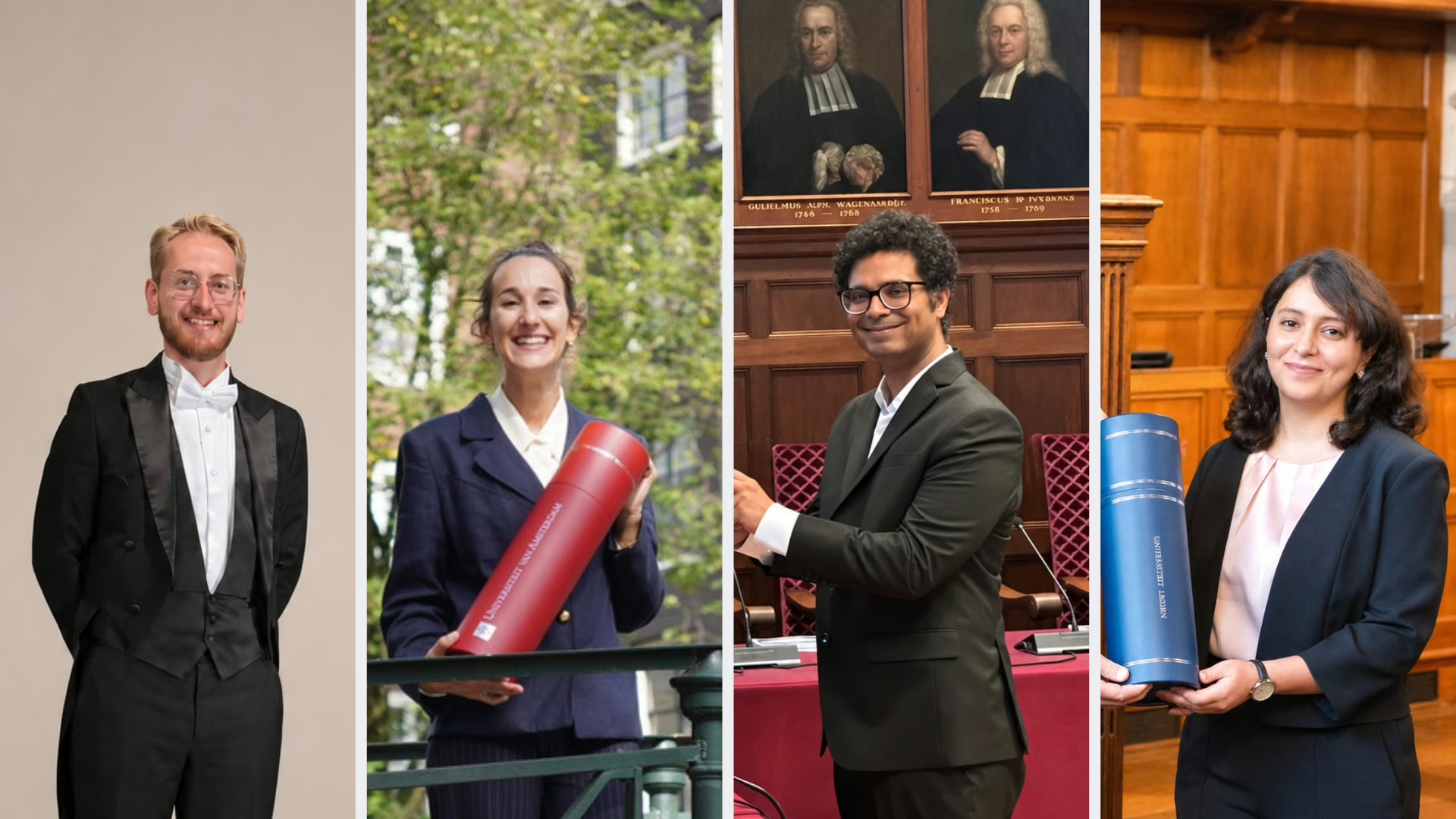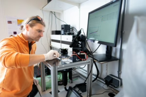
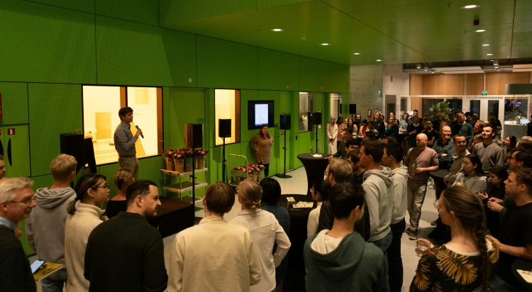
The event, which brought together past and present members of the AMOLF community, reflected the institute’s commitment to innovation and its people. Speeches highlighted the technical advancements of the upgraded NanoLab and Hans Zeijlemaker’s pivotal role in shaping AMOLF’s scientific facilities and culture.
A world-class facility reimagined
Ewold Verhagen, group leader and scientific coordinator of the NanoLab, opened the event by spotlighting the cutting-edge upgrades. “Nanostructures are central to the research at AMOLF and that of the many external users of the NanoLab. To remain at the forefront, we need to offer state-of-the-art facilities and exceptional support,” he explained. “The renovation expanded the facility. It also improved the ventilation systems and the overall cleanliness. The extra space and more efficient layout allows us to carry out significant investments within the Quantum Delta NL growth fund program. As part of the national facility NanoLabNL, we are installing advanced tools for atomic-precision deposition and 3D printing of nanoscale structures, among many other things.”
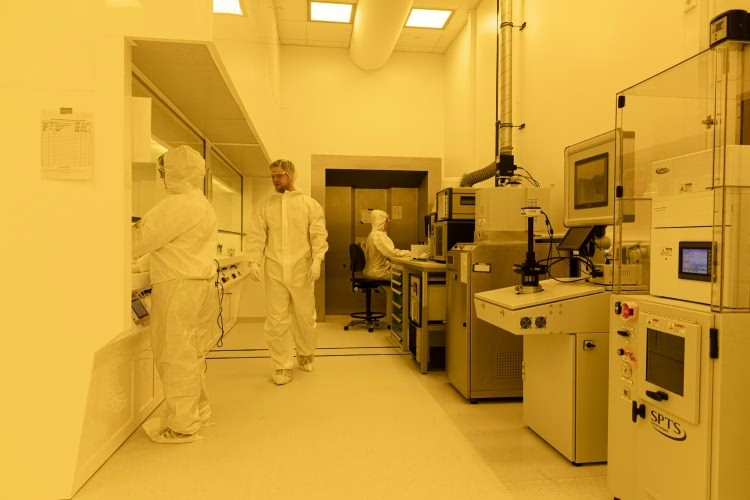
Institute manager Paula van Tijn emphasized the collaborative nature of the project. “This renovation was achieved remarkably quickly, despite technical challenges. It’s now a resource not only for AMOLF but also for external users from universities and companies, fostering new research and innovation. The upgraded NanoLab underscores AMOLF’s commitment to maintaining facilities that enable world-class science and support interdisciplinary collaboration.”
Honoring a legacy of excellence
The celebration also marked the retirement of Hans Zeijlemaker, whose contributions span decades of transformative change at AMOLF. Albert Polman, group leader and former director of AMOLF, shared precious memories of Hans’ early days. “As one colleague humorously noted, Hans can say things in a very nice way, sometimes not very precise because he wants to stay friendly. Despite suggestions to adopt a stricter approach, Hans stood by his own style, which proved to be right after all,” Albert said.
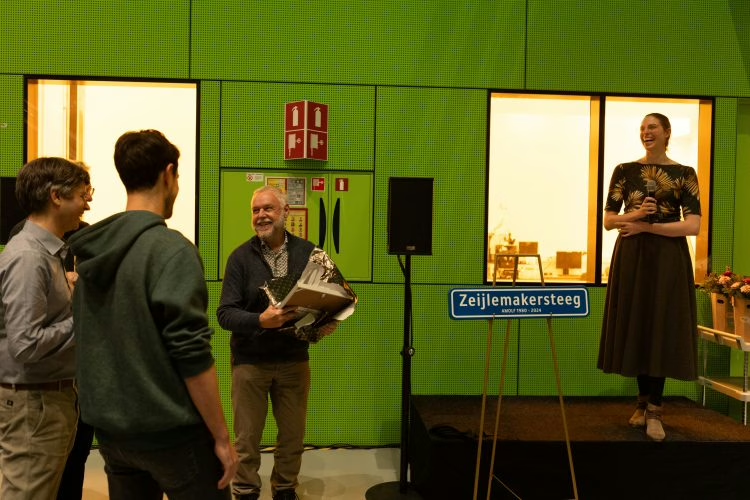
An absolute highlight of the ceremony was the unveiling of a custom-made street sign, ‘Zeijlemakersteeg’, to be displayed in the NanoLab. “Hans, this is a permanent reminder of your immense contributions and the legacy you leave behind,” Ewold said. Hans’ leadership style also received warm tributes. Colleagues recalled his balance of kindness and firmness, earning him respect and admiration across the institute.
Memorable farewell gifts
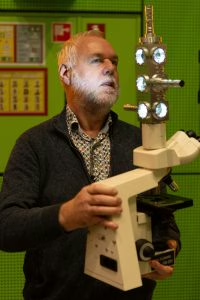
Isabelle Palstra, Hans’ successor as NanoLab head, shared her personal gratitude. “As a PhD student, I always felt supported by Hans, who patiently guided us no matter how often we needed help. We have two special gifts for you, that connect to your interests in both modern nanofabrication and historical lab equipment.”
Hans was presented with a working microscope, integrated with a replica of a scanning tunneling microscope, accompanied by a mosaic of microscopic photographs of Hans and his colleagues. And there was another gift: a hologram from the Dutch Holographic Laboratory. On this hologram, through a clever photographic technique, you can see a microscope where you can look through the holographic lens to see a computer chip.
Moved by these gestures, Hans expressed his gratitude. “These gifts are extraordinary. How did you manage to get these? These will get a very special place. Thank you all so much!”
A fond farewell and a bright future
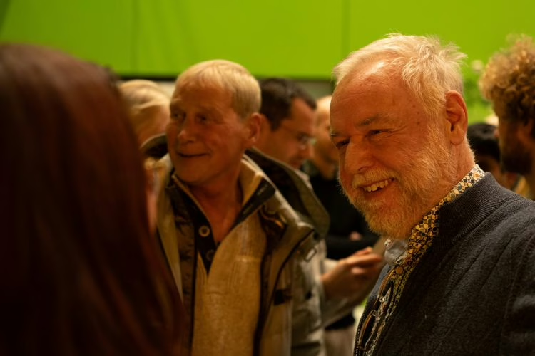
In his closing remarks, Hans reflected on his years at AMOLF, sharing anecdotes and advice. “Take time for the people around you – they are invaluable. And have fun!”
The ceremony concluded with Ewold Verhagen inviting everyone for drinks to celebrate both the new NanoLab and the beautiful memories of Hans Zeijlemaker.
AMOLF’s NanoLab
Do you have questions about AMOLF’s new NanoLab? Please contact Isabelle Palstra, head of AMOLF NanoLab Amsterdam (email: I.Palstra@amolf.nl).