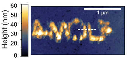
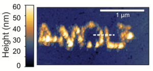
The copper clusters on the surface of the gold plate form the letters AMOLF (see image). These are invisible to the naked eye, because the letters are just a few hundred nanometers in size. However, the image is clearly visible through the microscope used to write the letters. Mark Aarts, PhD student in the 3D-Photovoltaics group, used this atomic force microscope (AFM) to manipulate dissolved copper ions to form these letters.
He can use the technique to draw any desired shape on a surface. The technique is suitable for the production of a new generation of nano-architectured solar cells, which capture sunlight in vertical nanostructures, such as wires, cones or perhaps even tree-shaped elements. Group leader Esther Alarcón explains: “In traditional solar cells, the light falls on the topmost horizontal layer; it gets darker as the depth in the material increases. In 3D solar cells, instead of just the top layer, the entire volume of the material is active.” One of the challenges is developing a new technique to directly produce nanowires from the bottom up with the help of electrochemical processes, instead of cutting them out of a larger piece of material. That is precisely what Aarts is working on.
Drawing with copper
Aarts uses a simple electrochemical reaction that one could perform in the kitchen with a clear blue solution of copper sulphate in a glass and two paperclips as electrodes. When a voltage is applied to the paperclips, copper deposits on one of them.
The same happens at the nanoscale in the AFM. A tiny platinum needle, 50 nanometers in diameter, moves over a surface like the needle of a record player moving over a record. In this experiment, this tip acts as the one paperclip, and a small gold plate (or the chip) on which the structure is drawn acts as the other paperclip. The entire setup is suspended in a copper-sulphate solution. If a voltage is applied across the electrodes, then copper deposits precisely where the tip is located on the gold surface. If the tip is moved, then the copper deposits slightly further up. With this approach, electrochemistry can be used to draw a pattern on a chip using an AFM.
Double layer
It soon became clear that the electrochemical process at the nanoscale did not proceed in the same way as at the kitchen table scale. For example, to his surprise, Aarts saw that more copper was deposited on the surface at lower concentrations of the copper sulphate solution. At high concentrations it was even impossible to write. However, tapping on the surface with the AFM tip did work well. That was necessary because without this tapping, no copper was formed. A fundamental process underlies this, Aarts explains. “A layer with the opposite charge always forms around a charged electrode. This ‘double layer’ also forms around our AFM tip and the gold electrode, and that prevents the copper reaction from taking place. That is surprising, because at the kitchen table scale, the double layer is what facilitates the reaction. By tapping the tip on the surface, the double layer is broken, which allows the reaction to take place locally.”
On to solar cells
Aarts is pleased with the successful production of 3D patterns using an AFM and an electrochemical reaction. The concentration effect and the need to tap have never previously been observed, the researcher says. “The double layer is one of the most important phenomena in electrochemistry, but we do not yet fully understand it. This knowledge could be important for the development of improved batteries or electrocatalysis.”
The structures that Aarts currently draws are about 50 nanometers in size, because that is the dimension of the AFM tip. However, smaller would be better. “We think that we could easily use a smaller tip to draw even smaller structures.”
The researchers’ dream is to produce solar cells using this technique. This will require the structures to be higher. “Increasing the height in a controlled manner is still difficult,” says Aarts, and so they are working on that. Ultimately, the production of solar cell will require structures built from several materials, such as gallium and arsenide, which combined form the best solar cells. “With electrochemistry, we can easily apply materials simultaneously or in sequence. Within the group we are also investigating these processes, and we hope to combine it all in the future.”
Reference
M. Aarts and E. Alarcón-Llado, Directed nanoscale metal deposition by the local perturbation of charge screening at the solid-liquid interface, Nanoscale (2019), DOI 10.1039/c9nr05574f