
AMOLF NanoLab Amsterdam
Nanolab equipment
AMOLF NanoLab Amsterdam is a facility for materials fabrication and characterization down to the nanometer scale. It aims to provide state-of-the art opportunities in nano research, servicing the scientific and engineering community within the greater Amsterdam area.
Facilities & Capabilities
AMOLF NanoLab Amsterdam includes an ISO class 5 cleanroom with facilities for optical- and electron beam lithography and plasma etching, a facility for thin film deposition, and innovative optical tools for nanofabrication, manipulation and analysis.
Researchers have access to a wide range of fabrication and inspection techniques in cleanroom environments, such as: Electron Beam Lithography, NUV lithography, two-photon lithography, FIB milling/deposition, EBID, reactive ion etching, thin film deposition, rapid thermal annealing, FE-SEM, EDX, Cathode luminescence, AFM, STM, surface profiling, spectroscopic ellipsometry, optical microscopy.
Equipment
Electron microscopes
Scanning electron microscope
Thermo Fisher Scienctific Helios UX 5
High-resolution imaging with high materials contrast, equipped with EDX, STEM and a SPARC detector for elemental analysis, transmission imaging and cathodoluminescence measurements. It is also equipped with an ultra-fast beam blanker capable of reaching blanking speeds of 50 ns. This FIB/SEM is equipped with micromanipulators to create TEM lamellae.
- Electron source: Elstar column with Schottky Field Electron Gun (SFEG)
- Electron beam resolution:
- 30 kV in STEM: 0.6 nm
- 15 kV: 0.6 nm
- 1 kV (optimal WD): 0.7 nm
- 1 kV (coincident point): 1.2 nm
- 500 V with ICD detector: 1.0 nm
- Electron beam currents: 0.8 pA to 100 nA
- Electron beam acceleration voltage: 350 V to 30 kV
- Landing energy range: 20 eV to 30 keV
FIB source information
- FIB source: Phoenix column with gallium liquid metal ion source (Ga-LIMS)
- FIB resolution: 2.5 nm to 4.0 nm depending on method
- FIB beam currents: 1pA to 65 nA
- FIB acceleration voltage: 500 V to 30 kV
Detector information
- Elstar in-lens SE/BSE detector (TLD-SE, TLD-BSE)
- Elstar in-column SE/BSE detector (ICD)
- Elstar in-column BSE detector (MD)
- Everhart-Thornley SE detector (ETD)
- IR camera for viewing inside chamber
- In-chamber secondary electron and secondary ion detector (ICE)
- Nav-cam
- Retractable solid-state backscatter electron detector (DBS)
- Retractable STEM 3+ detector with BF/DF/HAADF segments (STEM)
- Integrated beam current measurment
- 60 mm² x-ray detector (EDS, EDX)
Gas-injection system information
- Gas injection systems:
- C
- SiO2
- W
- XeF2
- Base pressure: 2.6×10⁻⁶ mBar
- NanoBuilder software for advanced object design
- AutoScript 4 for Python based scripting
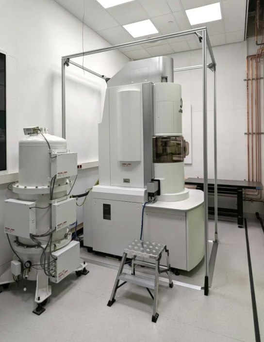 Transmission electron microscope
JEOL NeoARM TEM
Please visit [insert TEM link]
Scanning electron microscope
FEI Verios 460
High resolution scanning electron microscope with nanometer resolution.
- Sample size max. diameter 100 mm thickness 20 mm
- Schottky Field Electron Gun (SFEG)
- Electron Current 1pA to 22 nA
- sample landing energy range 50V30kV
- Electron energie monochromator for low energy spread < 0.2 eV
- 100 mm high precision 5 axis piezo stage sample
- NavCam sample navigation
- Energy Dispersive Spectroscopy (EDS) Oxford Xmax 80 mm^2 Silicon Drift Detector
- Elektron Backscatter Diffraction (EBSD) detector
- Homebuilt Electron Beam Induced Current Detector (EBIC) detector
- Plasma Cleaner
- Cryo Cleaner
- Electron detectors: ETD, TLD, MD, iCD, BSD, STEM
Etching
Plasma etching
Oxford PlasmaPro100 Cobra (Cobra)
A reactive ion etch system with inductively-coupled plasma. It has a combined load lock system via cleanroom interface for the RIE/ICP etch Cobra and the ICPCVD system
- gas inlet system for pressure control and gas mixtures
- gasses; CHF3, SF6, O2, Ar, C4F8, CF4, HBr and Cl2
- 300W RIE RF generator
- 3 kW ICP RF generator
- laser interferometer end point detector
- chiller temperature range 0°C to +80°C
- LN cryo-cooled electrically-heated temperature range -100°C to +400°C
- 4” wafer clamping with helium assisted heat transfer
- vacuum system; 1400 l/s turbo pump with a dry prevacuum pump
- scrubber for toxic gases
- It has a twin system, nicknamed the Viper
Integrated etch system that offers controlled vapor phase sacrificial oxide etching.
- KLA SPTS µEtch
- Single-wafer process tool
- Loader handles 100 –200 mm wafers
- Heated chamber and delivery line
- HF vapor flow control : 0 – 750 sccm
- Alcohol vapor flow control : 0 – 250 sccm ethanol vapor
- Process nitrogen flow control : 0 – 2 slm
- Operating pressure range 50 – 150 torr
Plasma etching
Oxford Plasmalab 80+
RF discharge tool for etching thin films. Some metals are allowed, after communication with the NanoLab staff.
- Process pressure 5-150 mbar
- Gas inlet system for process pressure control and gas mixtures
- Gasses; CHF3, SF6, O2, Ar
- Max 300 W for Reactive Ion Etching (RIE)
- Max 300 W for Inductive Coupled Plasma (ICP)
- ICP gives independent ion energy control
- Laser Interferometer endpoint detection
- Max size 90 mm diameter
Plasma etching
Oxford PlasmaPro 100 Cobra (Viper)
A reactive ion etch system with inductively-coupled plasma, with deep RIE options available such as Bosch and cryogenic etching.
- Gas inlet system for pressure control and gas mixtures
- Available gasses; CHF3, SF6, O2, Ar, C4F8, CF4, HBr and Cl2
- 300W RIE RF generator (including attenuator to go down to single Watt power output)
- 3 kW ICP RF generator
- Laser interferometer end point detection
- Chiller temperature range 0°C to +70°C
- LN cryo-cooled electrically-heated temperature range -100°C to +400°C
- 4” wafer clamping with helium assisted heat transfer
- Vacuum system; 1400 l/s turbo pump with a dry pre-vacuum pump
- Scrubber for toxic gases
- Close coupled gas pod for fast gas switching
- It has a twin system, nicknamed the Cobra
Xenon Difluoride Etching System
Homebuilt system
XeF2 etcher is a system to expose Si samples to XeF2 gas.
The etching is selective
Si : SiO2 => 500 : 1
Si : Si3N4=> 100: 1
Lithography
Direct Laser Writer
Heidelberg µMLA
A Tabletop maskless lithography tool
- 365 nm laser
- maximum substrate size: 6” x 6”
- minimum substrate size: 5 x 5 mm²
- maximum write area: 100 x 100 mm²
- substrate thickness: 0.1 to 12 mm
- encoder resolution: 20 nm, minimum feature size of 0.6 μm
- Raster mode and draw mode
Substrate Conformal Imprint Lithography
Suss MABA6 UV Mask aligner with SCIL
A tool for fabricating nanostructures in which a master pattern is replicated via a stamping process, by molding a liquid material in the inverse shape of the stamp, after which it is solidified. This technique combines the advantages of a soft stamp with a rigid glass carrier for low pattern deformation and best resolution for large area patterning.
- resolution down to sub 50nm on a 6” area
- high aspect ratio structures
- This tool is combined with the UV mask aligner
UV lithography
Suss MABA6 UV Mask aligner with SCIL
Optical lithography system. Pattern resolution of sub micron in contact mode.
- exposure lamp Hg 1000W
- normal exposure dose 25 mW/ cm2
- optics wavelength range UV300 280-350 nm (future UV 250 240-260 nm)
- exposure modes; proximity (1-300 mu gap), soft, hard and vacuum contact
- resolution depending on contact mode and mask <1 µm (future 0.5 µm)
- split field topside microscope with 5x, 10x and 20x objective
- bottom side microscope
- bottom and top alignment system accuracy 1 micron
- automatic wedge compensation
- mask holders; opening for 3”, 4”, 6” wafers and 30mm square
- sample chucks; 1”, 3” 4” and 6” wafers
- alignment stage; x +/10 mm Y +/5 mm theta 5°
- This tool is combined with the UV mask aligner
E-beam lithography
Voyager – Raith
Electron beam lithography system for high-resolution patterning
- Universal sample holder for small sample pieces up to 100mm 10mm max height
- Electron beam energy 10 – 50kV
- Beam current range 50 pA – 40 nA
- Beam size < 2.5 nm diameter at 50 kV
- Minimum feature size 20 nm in high resolution positive resist
- Stage range x=150 by y=150mm z=20 mm
- Mark recognition gives overlay accuracy of <35 nm
- GDSII format viewer and editor
- Import AutoCAD DXF,bitmap, ASCII or CIF format converted to GDSII
- Traxx and Periodixx software option
- FBMS and MBMS software option
Material characterisation
Atomic Force Microscopy
Bruker Dimension FastScan
An atomic force microscope system
- Sample size 210mm diameter 15mm thick
- Stage movement 150mm x 180mm with 2-3 micron resolution
- Video optics with zoom 130-1040 micron viewing area
- Piezo scan head range; 35 micron x-y and 3 micron in z
- Contact and tapping mode
- Peak force tapping mode
Electron beam physical vapor deposition
Polyteknik Flextura M506 E
Tool for physical vapor deposition of different materials. You can contact the NanoLab staff about available materials. The system is built according to our specifications by Polyteknik.
- Sample size diameter 4” max 4mm thick
- Load lock with separate turbo-pump
- Base pressure ~10-8 mbar (high vacuum; 400 l/s turbo, dry roughing pump)
- Ar etching gas, reactive gas evaporation with N2 and O2
- E-beam 10 kV, 500 mA evaporation source with 8 rotatable crucibles
- 2 thermal sources
- Co-evaporation
- Source to substrate distance 500mm
- 2 Quartz thickness monitors
- Sample heating till 400 °C
- Sample rotation, 360°
- Shutter system for sources and sample
- Linear shutter 100mm resolution 10µm
- Automated recipe driven software
Thin film analyzer
Filmetrics F20 UVX
Tool to measure material thickness and optical constants. Commonly analysed films include oxides, nitrides, resist, poly silicon and optical coatings.
- Sample size max. diameter 150 mm thickness 20 mm
- Reflection measurement 1.5 mm spot size
- High power UV-VIS fiber light source Hamamatsu model L10290
- D2 Lamp + Halogeen
- Scan range 190-1100 nm
- Measured thickness range 1 nm – 40 µm accuracy 1nm
- 50 nm minimal thickness to measure n & k
Nanoscale IR imaging
Neaspec – IR-neaSCOPE
Nanoscale infrared (IR) imaging and spectroscopy tool based on probing laser-induced
photothermal expansion with an AFM tip. Designed for nanoscale analysis that only requires measurements of IR absorbance. It detects laser-induced photothermal expansion in the sample using mechanical AFM-IR detection.
Sample preparation
E-beam lithography preparation software
GenISys Beamer
Software that allows the user to correct their e-beam exposure pattern process effects, electron scattering effects, and tool artifacts which would otherwise result in non-ideal pattern transfer.
- Optimized field and shot placement
- Writing order control and advanced writing strategies
- Library of comprehensive layout processing functions
- Integrated layout editor
- Built-in Viewer for immediate inspection, verification, and measurement of patterns
- Proximity and process effect correction tools
- Electron-beam simulation of absorbed energy and resist contours
Plasma cleaner
Diener Electronic Pico QR-200-PCCE
- 999% O2 gas
- 300 Watt 13,56 MHz
- Vacuum chamber with hinged door Ø 130 mm (5.1“), L 300 mm (11.8“) or 600 mm (23.6“)
Profilometer
KLA Tencor Stylus Profiler P7
Step height measurement tool for 2D and 3D measurements of step heights, surface roughness, sample stress, and sample bowing.
- Minimum substrate size: 3 x 3 mm
- Maximum substrate size: 150mm
- 2-micron radius 60 cone degree angled tip
- 5 – 50 mg stylus constant force
- Vertical resolution 0.4 nm
- Horizontal resolution 25 nm
Rapid thermal processor
AnnealSys AS-one 100
A rapid thermal annealing tool
- Max temperature 1450 °C
- Max hold times:
- 30 s at 1450 °C
- 10 minutes at 1200 °C
- 30 minutes at 1100 °C
- Reliable temperature ranges:
- RT – 1000 °C (using thermocouple)
- 150 – 1100 °C (using pyrometer 2)
- 300 – 1450 °C (using pyrometer 1)
- Max 150 °C/s ramp speed.
- Fast cooling option (uncontrolled and only without thermocouple).
- Pressure range: 5E-6 – 1000 mBar.
- Available gases:
- Oxygen (2000 sccm)
- Nitrogen (2000 sccm)
- Argon (2000 sccm)
- 5% Hydrogen in Nitrogen (1000 sccm)
Supercritical point dryer
Autosamdri 815 serie B
- Sample size max 30mm
- Sample holder for max 12X12mm and 10x10mm on site.
Vacuum oven
SalvisLab Vacucenter VC 20
- The vacuum oven is used to dry and anneal material under vacuum.
- range RT – 200°C
- vacuum variable with lowest pressure 10^-2 mbar
- venting with nitrogen
- programmable
Wet benches
Arias – custom build
Arias downflow wet benches for general purpose chemical work, both organic and inorganic. They both have a perforated working surface and a HEPA filtered down flow unit.
Additional equipment for use inside the wet benches:
- Nitrogen gun
- Demineralized water gun
- Branson 2800 Ultrasonic cleaning tank 40 kHz max 70 °C
- Sonosys Megasonic MSA-1800-4 1.8 MHz max 90 °C
- Heating plates
Thin film deposition
Atomic layer deposition
Veeco Fiji 2G
A tool for highly controlled conformal material deposition
- Thermal and plasma ALD
- Maximum substrate size 200 mm
- Available precursors.
- (Trimethyl)methylcyclopentadienylplatium (MPcPtMe3)
- Bis(diethylamino)silane (BDEASi)
- Cyclopentadienylindium (CpIn)
- Diethylzinc (DEZn)
- Tetrakis(dimethylamino)hafnium (TDMAHf)
- Tetrakis(dimethylamino)tin (TDMASn)
- Tetrakis(dimethylamino)titanium (TDMATi)
- Trimethylaluminum (TMA)
- If your desired precursor isn’t present, you can request it with the AMOLF NanoLab staff.
Electron beam physical vapor deposition
Polyteknik Flextura M506 E
Tool for physical vapor deposition of different materials. You can contact the NanoLab staff about available materials. The system is built according to our specifications by Polyteknik.
- Sample size diameter 4” max 4mm thick
- Load lock with separate turbo-pump
- Base pressure ~10-8 mbar (high vacuum; 400 l/s turbo, dry roughing pump)
- Ar etching gas, reactive gas evaporation with N2 and O2
- E-beam 10 kV, 500 mA evaporation source with 8 rotatable crucibles
- 2 thermal sources
- Co-evaporation
- Source to substrate distance 500mm
- 2 Quartz thickness monitors
- Sample heating till 400 °C
- Sample rotation, 360°
- Shutter system for sources and sample
- Linear shutter 100mm resolution 10µm
- Automated recipe driven software
Chemical vapor deposition
Oxford PlasmaPro100 ICPECVD
Inductively coupled plasma-enhanced chemical vapor deposition tool. Allows for the deposition of thin conformal layers of different materials
- gas control system for pressure controle and gas mixtures by flow gasses; SiH4, Ar, CH4, N2O, O2, N2, H2, SF6
- 300W RF generator
- 3 kW ICP RF generator
- Electrode temperature range 5°C to +400°C
- 4” wafer clamping with helium assisted heat transfer
- vacuum system; 1600 l/s turbo pump with a dry prevacuum pump
- scrubber for toxic gases
- combined loadlock system via cleanroom interface for the RIE/ICP etch Cobra and the ICPCVD system
–
Sputter system physical vapor deposition
Polyteknik Flextura M506 S
Tool for sputtering different materials. You can contact the NanoLab staff about available materials. The system is built according our specifications by Polyteknik.
- Max sample diameter 4”, max 4mm thick
- Load lock
- Base pressure ~10-8 mbar (high vacuum; 400 l/s turbo, dry roughing pump)
- Ar sputter gas, reactive gas N2 and O2
- 4 Polyteknik 3” Magnetrons
- 300W RF power supply
- 2kW DC, uni or bipolar pulse mode power supply
- Co-evaporation possible
- Quartz thickness monitor
- Sample heating till 400 °C
- Sample rotation, 360°
- Shutter system for sources and sample
- Automated recipe driven software
Notes:
- Use of adhesives to fix sample(s) is prohibited.
- Use of new material only allowed after additional training, every material behaves different!
Vacuum coating system
Smurf (homebuilt)
Homebuilt fast thermal coating system, dedicated for high vapor pressure materials such as Pb, Bi, Zn and alike, materials not allowed in the other evaporators.
- Homebuilt system
- Base pressure 10^-6 mbar
- Resistance heating evaporation
- 1 crucible made out Al2O3, Quartz, BN, Ta, Mo, C or intermetallic
- Flexible sample mounting max 4” diameter
- Quartz thickness monitor
Spin coater
CEE Apogee 200 Spin coater
- Flat substrates up to 200 mm or fragments
- Substrate thickness max 12 mm
- spin speed 5000 rpm
- Yields uniform coating thickness up to 100 µm
- Only cleanroom standard resists are allowed!
- Allowed resists only:
| Common name | Official name |
| CSAR 62 or just CSAR | AR-P 6200 |
| Elektra 92 or just Elektra | AR-PC 5092 |
| HSQ | XR 1541 |
| IP-G | IP-G |
| IP-L | IP-L |
| Ma-N 1400 | Ma-N 1400 |
| Ma-N 2400 | Ma-N 2400 |
| OrmoComp | OrmoComp |
| PMMA | 495 PMMA |
| PMMA | 950 PMMA |
| PMMA (imprint) | mr-I PMMA 35k |
| S1800 | Shipley S1800 |
| SU-8 | SU-8 3000 |
Explicit permission from staff member necessary for any other materials
Spin coater
SPS Europe POLOS 200i
- Substrate size: 100 mm wafers
- Substrate thickness max 12 mm
- spin speed 5000 rpm
- Yields uniform coating thickness up to 100 micron
- Any coating may be applied in this tool
- Mobile system, must be set-up in a wet bench before use
–